Machine vision inspection system is applied to semiconductor–wafer appearance inspection
Due to the characteristics of the wafer, there are some difficulties to be solved in actual operation when using machine vision to detect it.
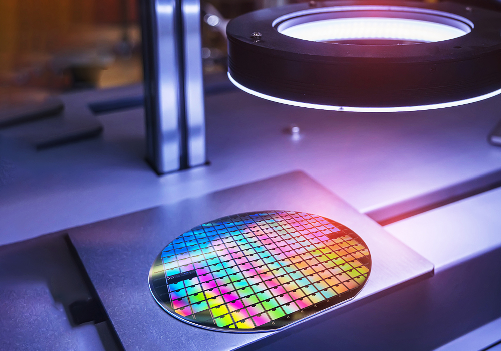
Silicon Wafers and Microcircuits with Automation vision sensor camera system control application
Characteristics of wafers:
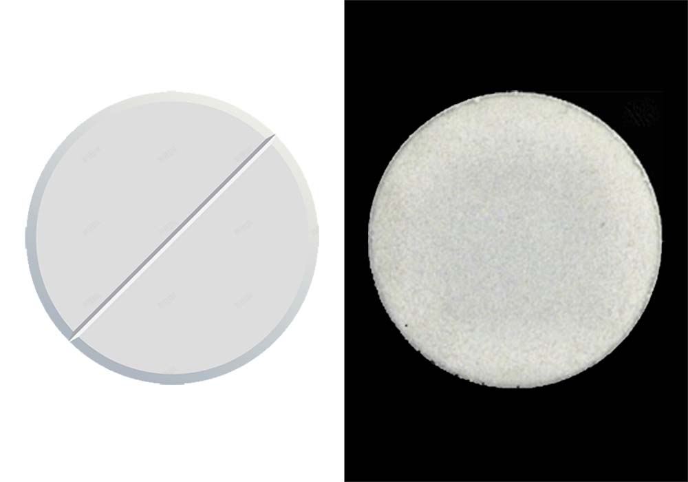
1. Complex surface reflection
The surface of the wafer is very smooth, like a mirror, reflecting the surrounding light. This brings challenges to image acquisition. Only through careful design of lighting and light source programming, reasonable image enhancement, etc., can images that can be used for inspection be obtained.
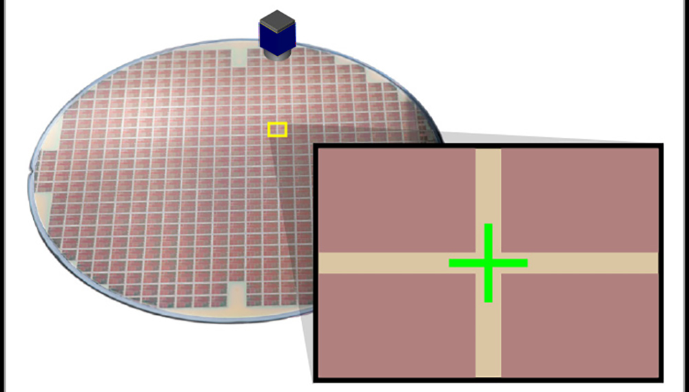
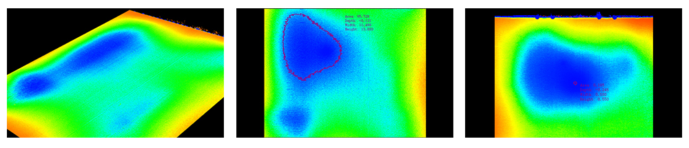
2. The size of the defects is tiny.
The defects on the surface of the wafer are often very small, as small as a few microns, and cannot be seen by the human eye. These tiny defects cannot be captured by ordinary cameras. High-resolution, high-sensitivity industrial cameras must be used, combined with the system’s algorithm to properly process the image, to identify these tiny defects.
3. High detection speed requirements
The wafer production speed on the production line is very fast. To achieve real-time image acquisition and analysis, detection system requirements are very high. Industrial cameras and algorithms must have high-speed performance.
4. The surrounding environment is easily disturbed.
Due to the smooth surface of the wafer, dust and vibration around it will affect image acquisition.
Detection system hardware configuration
Overall dimension: 900*800*1850mm
| No. | Name | Model | Quantity | Remark |
| 1 | Visual inspection software | Intsoft customized | 1 set | Data can be upload |
| 2 | Industrial computer | Intsoft customized | 1 set | |
| 3 | Monitor | PHILIPS 19 “LCD monitor | 1 set | |
| 4 | Industrial camera | Barsler industrial camera | 6 sets | |
| 5 | Industrial lens | FA High Definition Optical Industrial Lens | 6 sets | |
| 6 | Light source | Customized optical adaptive light source | 4 sets | |
| 7 | Inspection Platform | Professional Optical Glass Carrier | 1 set | |
| 8 | Servo Motor | Panasonic | 1 set | |
| 9 | Control System | Intsoft customized | 1 set | |
| 10 | PLC motion collaboration | Panasonic | 1 set |
Inspection process:
1. Loading: Fixing and positioning the wafer to the inspection area through a robotic arm
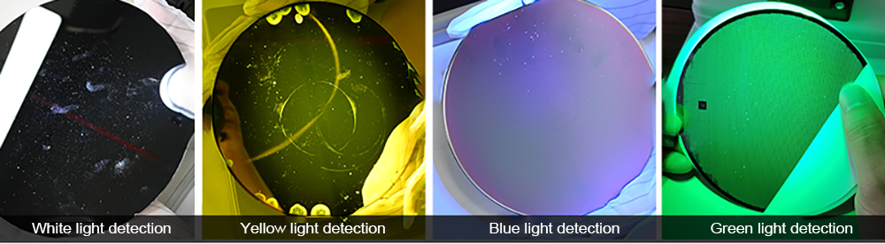
2. Image acquisition: Use programmable LED light source, multi-angle lighting, and high-resolution industrial camera to scan the wafer comprehensively and collect clear image data.
3. Image processing: Through the algorithm, the collected image is corrected by various parameters to facilitate the next step of image analysis.
4. Defect detection: Input processed image information into the visual analysis model. The trained visual analysis model can quickly identify various defects, such as cracks, dirt, black spots, etc., and generate corresponding instructions to sort out these defective products.
5. Dimension measurement: Measure the size and thickness of the wafer through an industrial camera, and generate corresponding instructions to sort out products that do not meet production standards.
6. Generate a report: The system will produce a detailed report that records the defect location, type, frequency, etc. in detail.
7. Data processing: This defect and dimension data will be saved and used as materials for automated AI training to improve the accuracy and speed of subsequent defect detection.
Point of attention:
1. Lighting
The deployment of light sources should be reasonable, and the quantity, angle, and brightness should be carefully adjusted to ensure that a shadow-free image is obtained.
2. Image processing
Depending on the actual lighting conditions and image characteristics, various image parameters should be adjusted to highlight defects.
3. Image analysis model
The defect detection training model based on deep learning requires a large number of defect sample training in the early stage, and later recognition will be more accurate and faster.
4. System integration debugging
The coordination of various hardware modules should be synchronized and tight so that the system can run smoothly and stably.