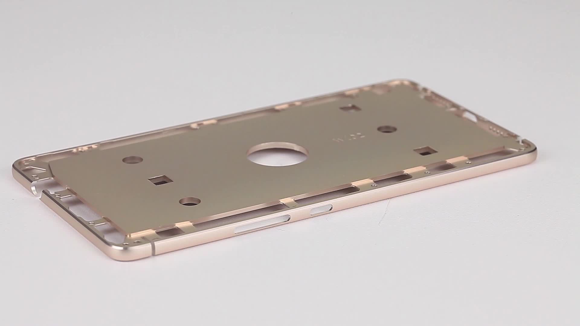
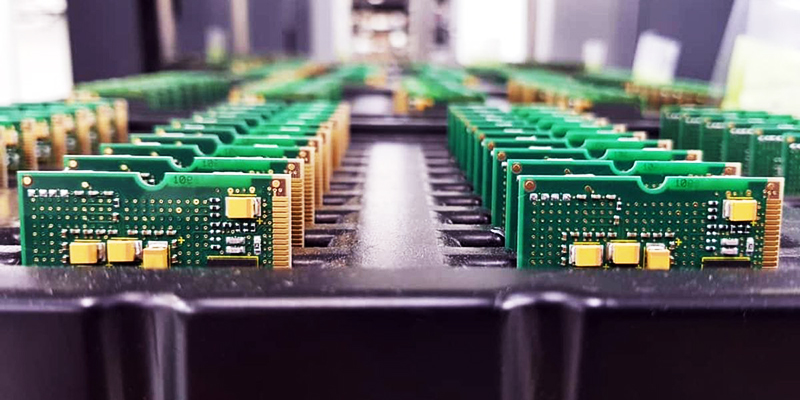
The importance of PCB(printed circuit board) in reality
In the world of modern electronic products, PCB (printed circuit board) is an important part of the composition of electronic products. PCB is equivalent to the human brain, a variety of functions of electronic products, such as switches, sound regulation, brightness adjustment, all through PCB modulation.
So how the quality of PCB will bring a very big impact on the long-term normal and reliable work of electronic products. Improving PCB quality is an important issue that electronic product manufacturers should pay sufficient attention to.
An excellent implementation of the solder paste printing process can be triggered by the connection of electronic circuits. In order to effectively solve this problem, many screen printing equipment manufacturers have adopted online machine vision inspection technology. The following are briefly introduced:
Industrial Camera Positioning and Inspection
In a typical online vision inspection application, an industrial camera is positioned above the circuit board to obtain an image of the printed position and send the relevant image to the processing system of the vision inspection device.
The image analysis software compares the acquired image with a reference image stored at the same location in the device memory.
This way, the system can confirm whether more or less solder paste has been applied. Similarly, the system can reveal whether the solder paste position on the pads is aligned correctly, and it can find out if there is any excess solder paste between the two pads to form a bridge-like connection. This problem is also commonly referred to as “bridging” by many manufacturers of printed circuit boards.
Detection of stencil gap
Detecting gaps in the stencil works similarly to the example shown above. When solder paste accumulates on the surface of the stencil, the vision system can detect if gaps are clogged with solder paste or if trailing is occurring. When defects are detected, the machine can immediately and automatically request a series of cleaning operations on the screen below, or alert the operator that a problem exists that needs to be repaired. The stencil detection also provides the user with very useful data on print quality and consistency.
A key feature of online vision systems is the ability to inspect PCB boards and pad surfaces that are highly reflective, as well as under uneven light conditions or conditions where dry solder paste structures make a difference.
Detection Process
As an example, HASL boards are generally characterized by uneven flatness, variable surface contours and reflective capabilities.
Proper lighting also plays a very important role in obtaining a high quality image.
The light must be able to “point” at the board’s datums and pads so that other invisible features become clearly recognizable shapes.
The next step is to use vision software rule systems to realize their full potential.

In some specific cases, vision systems can be used to detect the height or size of the solder paste volume on the pads, which may sometimes be done using only an offline detection system.
The use of this procedure means that a corresponding stacking degree is formed in a given printing template to confirm that the volume of solder paste on the same pads is missing or not.
In practice, detection can be divided into two main categories: detection of solder paste on PCB and detection of solder paste on printed stencil:
1. Detection of PCB
The main detect printing area, offset printing and bridging phenomenon. Print area detection refers to the area of solder paste on each pad. Excessive solder paste may cause the phenomenon of bridging, and too little solder paste can also cause the phenomenon of weak solder joints. Print offset is the detection of whether the amount of solder paste on the pads is different from the specified position. The detection of bridging phenomenon is to see if the solder paste between two neighboring pads exceeds the specific amount.
2. Print template detection.
Print template detection is mainly for the detection of blocking and trailing phenomenon. Blockage detection refers to the detection of solder paste whether it accumulates in the holes in the printing stencil. If the holes are clogged, too little solder paste may be applied to the next printing point. Detection of trailing refers to the detection of excessive solder paste accumulated on the surface of the printing stencil. This excess solder paste may be applied to the board where it should not be energized, causing electrical connection problems.
Online machine vision systems can benefit PCB manufacturers in a variety of ways. In addition to ensuring a high degree of solder joint integrity, it also prevents manufacturers from wasting money on board defects and resulting rework. Perhaps most importantly, it provides continuous process feedback, which not only helps manufacturers optimize the screen printing process, but also adds confidence in the process.