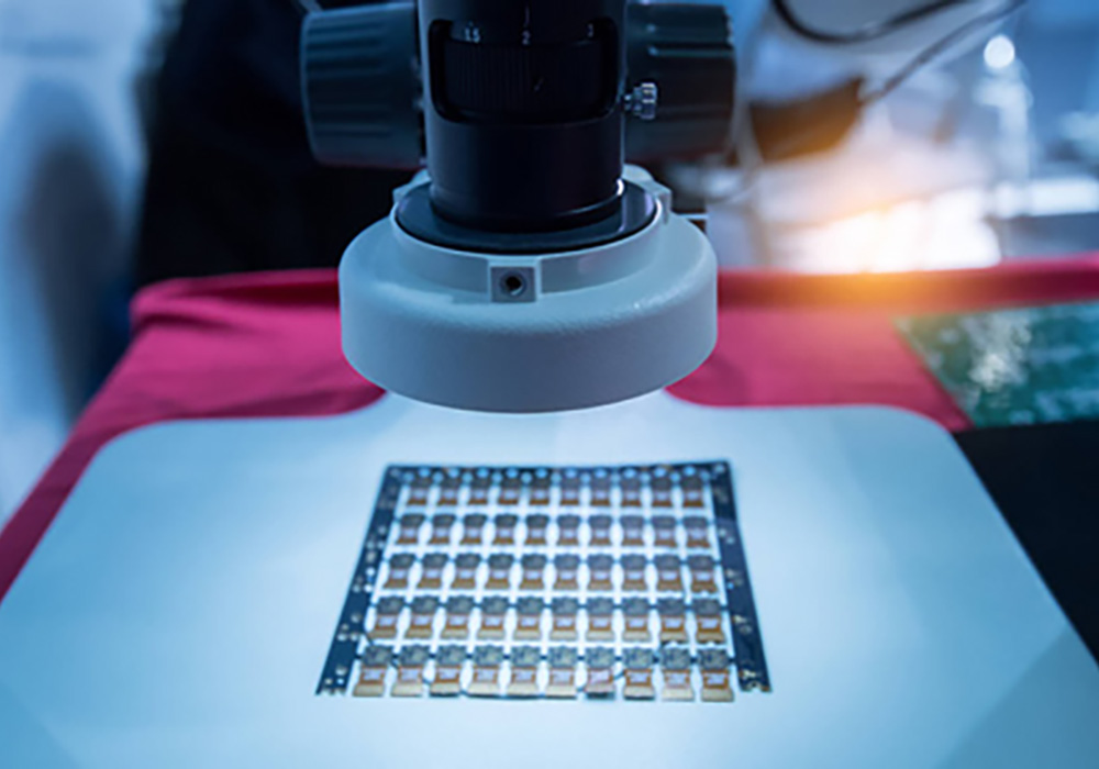
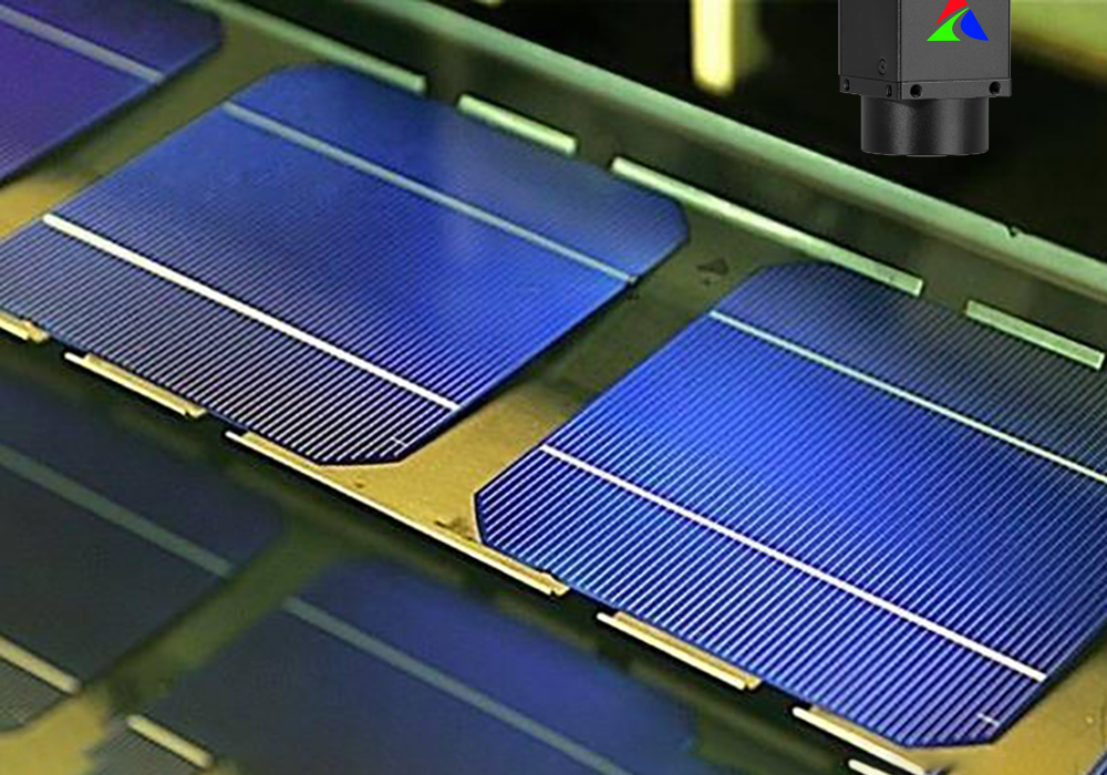
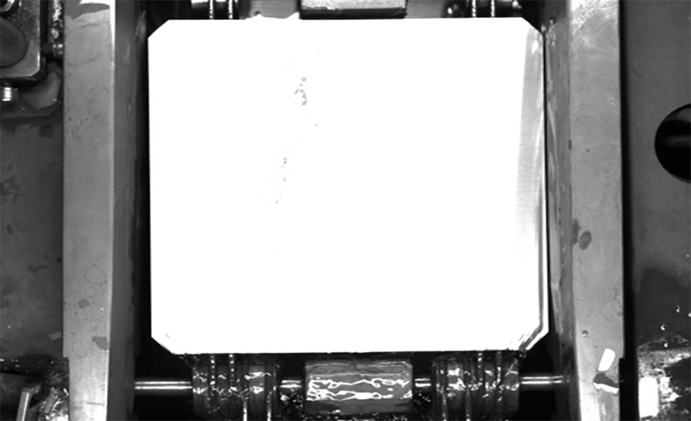
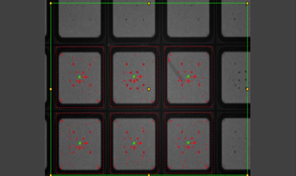
There are dozens of defects involved in the appearance inspection of solar silicon wafers, including cracks, broken edges, missing corners, dirt, etc. There are many inspection needs, and customers have high requirements for machine vision inspection. The repeatability accuracy needs to be ≤0.1mm, and the inspection width must also be customized according to the specific product. We need to find more effective ways to meet the inspection needs of different silicon wafer sizes while replacing people with machines.
Intsoft Tech inspection solution
1. One solution meets multiple inspection requirements: automatically matches silicon wafers of different sizes to meet large-scale capacity expansion needs.
2. Convenient data interaction: directly interact with PLC and write data to PLC data storage area, which is convenient and fast.
| Item | Tech parameter |
| Inspection area | 155*155 mm — 165*165mm |
| Inspection sides | Front and back |
| Speed | 80pcs/min |
| Resolution | 0.02mm(Longitudinal)0.02mm(transverse) |
| Min. Detectable point | 0.002 mm2 |
| Min. Detectable line | 0.02mm(width)* 1mm(length) |
| Min. Detectable color difference | 24 types |
| Defect type | Cracks, missing edges, bright lines, color difference, oxidation, scratches, black circles, oil stains, lattices, yellow spots, velvet, decrystalline, water marks, dirt, broken grids, leakage, etc. |
 Technical characteristics of the solar wafer visual inspection system
1. High detection accuracy, fine defect detection
2. The detection accuracy is up to 0.02mm, which can detect very fine defects.
3. Repeat positioning accuracy ≤ 0.1mm
4. Multiple color sorting types, up to 24 types
5. Based on the color difference of silicon wafers, silicon wafers are classified into 24 color differences.
6. Inspection speed increased: 3pcs/s